XCEL ASICs
Sarl
Accelerating High-Throughput Low-Power Silicon
THE PROBLEM
The Scaling Bottleneck in Advanced CMOS
As advanced CMOS implementation become increasingly wire-dominated, performance is limited not by logic density but by:
-
Routing congestion
-
Wire-dominated delay
-
Memory bandwidth constraints
-
Data-movement overhead
In highly parallel compute engines, these factors limit clock frequency, increase power consumption, and restrict scalability. Conventional architectures struggle to sustain tens of Gbps throughput within strict power and area budgets.
THE SOLUTION
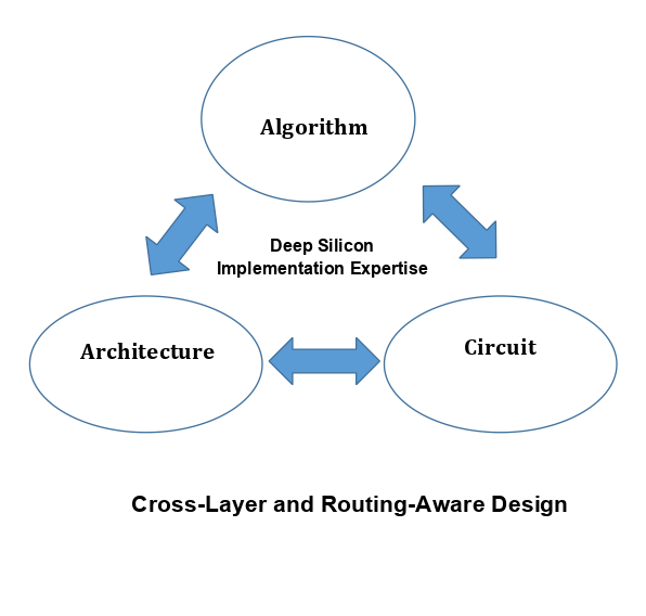
Routing-Aware Cross-Layer Co-Design
XCEL ASICs addresses these bottlenecks through tightly integrated cross-layer optimization that combines:
- Algorithm development
- Interconnect-aware architecture
- Memory-access restructuring
- Deep silicon implementation expertise
By co-optimizing algorithm, architecture, and implementation, we enable scalable ultra-high-throughput silicon optimized for performance, power, and area efficiency.
PRODUCTS
Our current portfolio includes high-performance error-correction IP cores engineered for advanced communication applications. These implementations are developed using routing-aware architectures, cross-layer co-design, and deep physical implementation optimization techniques that extend to other ultra-high-throughput communication and compute systems. Recent innovations include:
-
An ultra-high-throughput WiFi LDPC decoder — designed to meet next-gen connectivity demands,
-
An area-efficient high-throughput LDPC decoder for 5G-NR with full standard compliance,
-
A multi-Gbps LDPC decoder for WiGig (60 GHz) wireless systems,
-
An optimized 5G-NR polar decoder, engineered for performance and low latency.
Services:
-
ASIC development and FPGA prototyping for communication, AI, and DSP applications,
-
Simulation and verification of ASICs and standalone IP cores,
-
Synthesis, placement, and routing of digital blocks for ASIC tapeout,
-
Design, simulation, and implementation of digital communication, AI, or DSP systems.